(Singapore)

Product Summary
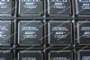
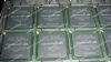
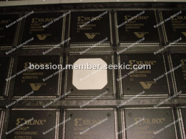
The XCV600-5HQ240I is an FPGA. It delivers high-performance, high-capacity programmable logic solutions. Dramatic increases in silicon efficiency result from optimizing the new architecture for place-and-route efficiency and exploiting an aggressive 5-layer-metal 0.22 µm CMOS process. These advances make the XCV600-5HQ240I powerful and flexible alternatives to mask-programmed gate arrays.
Parametrics
XCV600-5HQ240I absolute maximum ratings: (1)VCCINT, Supply voltage relative to GND: –0.5 to 3.0 V; (2)VCCO, Supply voltage relative to GND: –0.5 to 4.0 V; (3)VREF, Input Reference Voltage: –0.5 to 3.6 V; (4)VIN, Input voltage relative to GND Using VREF: –0.5 to 3.6 V; Internal threshold: –0.5 to 5.5 V; (5)VTS, Voltage applied to 3-state output: –0.5 to 5.5 V; (6)VCC, Longest Supply Voltage Rise Time from 1V-2.375V: 50 ms; (7)TSTG, Storage temperature (ambient): –65 to +150℃; (8)TJ, Junction temperature: +125℃.
Features
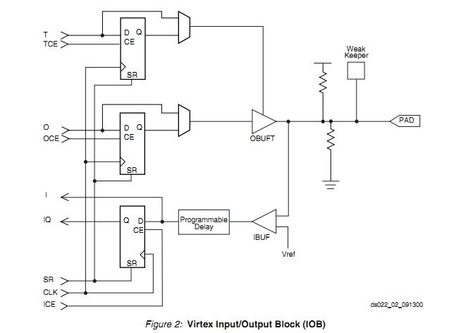
XCV600-5HQ240I features: (1)Fast, high-density Field-Programmable Gate Arrays: Densities from 50k to 1M system gates; System performance up to 200 MHz; 66-MHz PCI Compliant; Hot-swappable for Compact PCI; (2)Multi-standard SelectIO interfaces: 16 high-performance interface standards; Connects directly to ZBTRAM devices; (3)Built-in clock-management circuitry: Four dedicated delay-locked loops (DLLs) for advanced clock control; Four primary low-skew global clock distribution nets, plus 24 secondary local clock nets; (4)Hierarchical memory system: LUTs configurable as 16-bit RAM, 32-bit RAM, 16-bit dual-ported RAM, or 16-bit Shift Register; Configurable synchronous dual-ported 4k-bit RAMs; Fast interfaces to external high-performance RAMs; (5)Flexible architecture that balances speed and density: Dedicated carry logic for high-speed arithmetic; Dedicated multiplier support; Cascade chain for wide-input functions; Abundant registers/latches with clock enable, and dual synchronous/asynchronous set and reset; Internal 3-state bussing; IEEE 1149.1 boundary-scan logic; Die-temperature sensor diode; (6)Supported by FPGA Foundation and Alliance Development Systems; (7)Complete support for Unified Libraries, Relationally Placed Macros, and Design Manager; (8)Wide selection of PC and workstation platforms; (9)SRAM-based in-system configuration; (10)Unlimited re-programmability; (11)Four programming modes; (12)0.22 mm 5-layer metal process; (13)100% factory tested.
Diagrams
| Image | Part No | Mfg | Description |  |
Pricing (USD) |
Quantity | ||||
|---|---|---|---|---|---|---|---|---|---|---|
 |
 XCV600-5HQ240I |
|
IC FPGA 2.5V I-TEMP 240-HQFP |
Data Sheet |
Negotiable |
|
||||
| Image | Part No | Mfg | Description | |
Pricing (USD) |
Quantity | ||||
|
XCV600-4BG432C |
|
IC FPGA 2.5V C-TEMP 432-MBGA |
Data Sheet |
Negotiable |
|
||||
|
XCV600-4BG432I |
|
IC FPGA 2.5V I-TEMP 432-MBGA |
Data Sheet |
Negotiable |
|
||||
|
XCV600-4BG560C |
|
IC FPGA 2.5V C-TEMP 560-MBGA |
Data Sheet |
Negotiable |
|
||||
|
XCV600-4BG560I |
|
IC FPGA 2.5V I-TEMP 560-MBGA |
Data Sheet |
Negotiable |
|
||||
 |
XCV600-4FG676C |
|
IC FPGA 2.5V C-TEMP 676-FBGA |
Data Sheet |
Negotiable |
|
||||
|
XCV600-4FG676I |
|
IC FPGA 2.5V I-TEMP 676-FBGA |
Data Sheet |
Negotiable |
|
||||