Product Summary
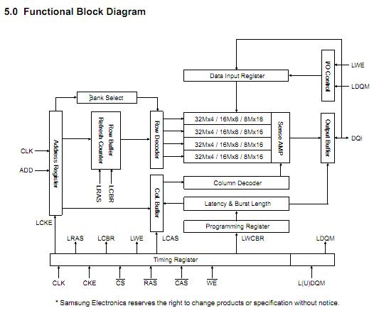
The K9HCG08U1M-PCB0 is a 536,870,912 bits synchronous high data rate Dynamic RAM organized as 4 x 33,554,432 words by 4 bits / 4 x 16,777,216 words by 8 bits / 4 x 8,388,608 words by 16 bits, fabricated with SAMSUNG’s high performance CMOS technology. Synchronous design allows precise cycle control with the use of system clock I/O transactions are possible on every clock cycle. Range of operating frequencies, programmable burst length and programmable latencies allow the same device to be useful for a variety of high bandwidth, high performance memory system applications.
Parametrics
K9HCG08U1M-PCB0 absolute maximum ratings: (1)Voltage on any pin relative to Vss, VIN, VOUT: -1.0 ~ 4.6 V; (2)Voltage on VDD supply relative to Vss, VDD, VDDQ: -1.0 ~ 4.6 V; (3)Storage temperature, TSTG: -55 ~ +150℃; (4)Power dissipation, PD: 1W; (5)Short circuit current, IOS: 50 mA.
Features
K9HCG08U1M-PCB0 features: (1)JEDEC standard 3.3V power supply; (2)LVTTL compatible with multiplexed address; (3)Four banks operation; (4)MRS cycle with address key programs; (5)All inputs are sampled at the positive going edge of the system clock; (6)Burst read single-bit write operation; (7)DQM (×4,×8) & L(U)DQM (×16) for masking ; (8)Auto & self refresh; (9)64ms refresh period (8K Cycle); (10)54pin TSOP II Pb-Free package; (11)RoHS compliant.
Diagrams

 (Singapore)


