Product Summary
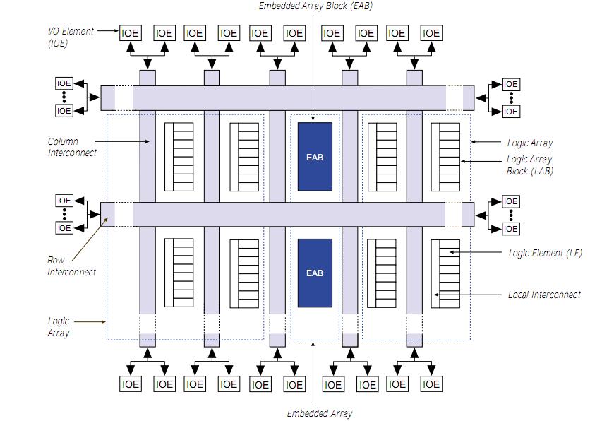
The EP1K50FC484-3N is a Programmable Logic Device. It provides a die-efficient, low-cost architecture by combining look-up table (LUT) architecture with EABs. Based on reconfigurable CMOS SRAM elements, the EP1K50FC484-3N architecture incorporates all features necessary to implement common gate array megafunctions, along with a high pin count to enable an effective interface with system components. The ability to reconfigure EP1K50FC484-3N enables complete testing prior to shipment and allows the designer to focus on simulation and design verification.
Parametrics
EP1K50FC484-3N absolute maximum ratings: (1)Supply voltage With respect to ground:-0.5 to 3.6V, -0.5 to 4.6V; (2)DC input voltage:-2.0 to 5.75V; (3)DC output current, per pin:–25 to 25 mA; (4)Storage temperature:–65℃ to 150℃; (5)Ambient temperature:–65℃ to 135℃; (6)Junction temperature:135℃.
Features
EP1K50FC484-3N features: (1)Enhanced embedded array for implementing megafunctions ; (2)such as efficient memory and specialized logic functions ; (3)Dual-port capability with up to 16-bit width per embedded array block (EAB); (4)Logic array for general logic functions; (5)10,000 to 100,000 typical gates; (6)Up to 49,152 RAM bits (4,096 bits per EAB, all of which can be used without reducing logic capacity); (7)Cost-optimized process; (8)Low cost solution for high-performance communications applications; (9)Built-in Joint Test Action Group (JTAG) boundary-scan test(BST) circuitry compliant with IEEE Std. 1149.1-1990, available without consuming additional device logic.; (10)Operate with a 2.5-V internal supply voltage; (11)In-circuit reconfigurability (ICR) via external configuration devices, intelligent controller, or JTAG port; (12)ClockLockTM and ClockBoostTM options for reduced clock delay, clock skew, and clock multiplication; (13)Built-in, low-skew clock distribution trees; (14)100% functional testing of all devices; test vectors or scan chains are not required; (15)Pull-up on I/O pins before and during configuration; (16)Individual tri-state output enable control for each pin; (17)Open-drain option on each I/O pin; (18)Programmable output slew-rate control to reduce switching noise; (19)Clamp to VCCIO user-selectable on a pin-by-pin basis; (20)Supports hot-socketing.
Diagrams

| Image | Part No | Mfg | Description |  |
Pricing (USD) |
Quantity | ||||||
|---|---|---|---|---|---|---|---|---|---|---|---|---|
 |
 EP1K50FC484-3N |
 |
 IC ACEX 1K FPGA 50K 484-FBGA |
 Data Sheet |

|
|
||||||
| Image | Part No | Mfg | Description |  |
Pricing (USD) |
Quantity | ||||||
 |
 EP1K100FC256-1 |
 |
 IC ACEX 1K FPGA 100K 256-FBGA |
 Data Sheet |

|
|
||||||
 |
 EP1K100FC256-1N |
 |
 IC ACEX 1K FPGA 100K 256-FBGA |
 Data Sheet |

|
|
||||||
 |
 EP1K100FC256-2 |
 |
 IC ACEX 1K FPGA 100K 256-FBGA |
 Data Sheet |

|
|
||||||
 |
 EP1K100FC256-2N |
 |
 IC ACEX 1K FPGA 100K 256-FBGA |
 Data Sheet |

|
|
||||||
 |
 EP1K100FC256-3 |
 |
 IC ACEX 1K FPGA 100K 256-FBGA |
 Data Sheet |

|
|
||||||
 |
 EP1K100FC256-3N |
 |
 IC ACEX 1K FPGA 100K 256-FBGA |
 Data Sheet |

|
|
||||||
 (Singapore)


